|
Fujitsu Technology Bonds Single-crystal Diamond and SiC at Room Temperature; Enables Boost to Radar Performance
In world's first such technology, cooling efficiency improved, radar's observable range enhanced about 1.5 times on increased GaN-HEMT power-amp transmitter output
TOKYO, 2017年12月07日 - (JCN Newswire) - Fujitsu Limited and Fujitsu Laboratories Ltd. today announced development of the world's first technology for bonding single-crystal diamond to a silicon carbide (SiC)(1) substrate at room temperature. Using this technology for heat dissipation in a high-power gallium nitride (GaN)(2) high electron-mobility transistor (HEMT)(3) enables stable operations at high power levels. Application of this technology is expected to significantly enhance the performance of weather radars and wireless communications.
 | | Figure 1: Structure of conventional GaN-HEMT power amp |
 | | Figure 2: Structure of GaN-HEMT power amp with bonded diamond |
 | | Figure 3: Diamond cross section after Ar beam exposure |
 | | Figure 4: A GaN-HEMT/SiC substrate with diamond bonded using this technology |
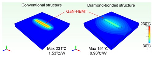 | | Figure 5: Simulated comparison of heat in 200W-class GaN-HEMT power amps |
Boosting range and power in radar and wireless communications also increases the heat produced by devices, which adversely affects their performance and reliability. This creates a need to efficiently carry device heat to a cooling structure. Single-crystal diamond is known to have good thermal conductivity, but with existing technologies, the argon (Ar) beams used to remove impurities in the manufacturing process create a low-density damaged layer on the surface, which weakens bonding strength. Also, bonding with an insulating film such as silicon nitride (SiN) impairs thermal conductivity due to SiN's thermal resistance.
Now, by protecting the surface of the diamond with an extremely thin metallic film, Fujitsu and Fujitsu Laboratories succeeded in preventing the formation of the damaged layer and bonding single-crystal diamond to a SiC substrate at "room-temperature bonding"(4). Simulations using actual measurements of thermal parameters have confirmed that devices using this technology would lower thermal resistance to 61% of existing ones.
This technology promises GaN-HEMT power amps for transmitters to operate at higher power, and increase the observable range by roughly 1.5 times when applied to systems such as weather radar.
This research was conducted in part with support from the Innovative Science and Technology Initiative for Security, established by the Acquisition, Technology & Logistics Agency (ALTA), Japan Ministry of Defense.
Details of this technology are being presented at the IEEE Semiconductor Interface Specialists Conference (SISC2017), running December 6-9 in San Diego, U.S.
Background
In recent years, high-frequency GaN-HEMT power amps have widely been used for long-range radio applications, such as radar and wireless communications. They are also expected to be used in weather radar that observes localized heavy rains, for example, or in the forthcoming 5G millimeter-band mobile communications protocols. For these types of radars or wireless communications using the microwave to millimeter-wave bands, by raising the output of the GaN-HEMT power amps used for transmissions, the distance that radio waves can propagate will allow the expansion of the observational range of radar while enabling longer and higher capacity communications. This is why GaN-HEMT power amps with higher power output are desirable.
http://www.acnnewswire.com/topimg/Low_FujitsuSiCFig1.jpg
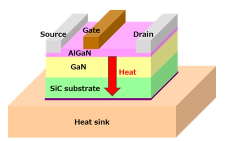
Figure 1: Structure of conventional GaN-HEMT power amp
Issues
In GaN-HEMT power amps, some of the input power is converted to heat (Figure 1). This heat is dispersed into the SiC substrate, and is carried away by a cooling structure (heat sink). Although the SiC substrate has relatively high thermal conductivity, a material with even better thermal conductivity will be needed for devices with increasingly higher power output to efficiently carry device heat to the cooling structure.
Single-crystal diamond has extremely good thermal conductivity-almost five times that of a SiC substrate-and is known as a material that can efficiently spread heat. In order to bond a single-crystal diamond to a device as a cooling material, normal production processes use an Ar beam to remove impurities, which produces a low-density damaged surface that weakens the bonds the single-crystal diamond can form. Moreover, using SiN or other insulating films for bonding interferes with thermal conductivity due to SiN's thermal resistance.
About the Technology
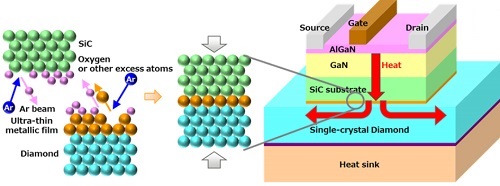
Fujitsu and Fujitsu Laboratories have succeeded in developing the world's first technology for room-temperature bonding onto a SiC substrate single-crystal diamond, used for high-efficiency cooling of GaN-HEMT power amps. These two hard materials have different coefficients of thermal expansion (Figure 2).
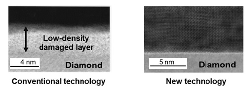
To prevent the Ar beam from forming a damaged layer on the diamond surface, the companies developed a technique that protects the surface with an extremely thin metallic film before it is exposed to the Ar beam. In order to ensure the surface is planar, for good bonding at room temperature, the metallic film is held to a thickness of 10 nm or less. This technology was confirmed to prevent the formation of the damaged layer on the diamond surface after Ar beam exposure (Figure 3), resulting in improved bonding strength and single-crystal diamond bonded at room temperature to a SiC substrate for GaN-HEMT.
http://www.acnnewswire.com/topimg/Low_FujitsuSiCFig2.jpg
Figure 2: Structure of GaN-HEMT power amp with bonded diamond
http://www.acnnewswire.com/topimg/Low_FujitsuSiCFig3.jpg
Figure 3: Diamond cross section after Ar beam exposure
http://www.acnnewswire.com/topimg/Low_FujitsuSiCFig4.jpg
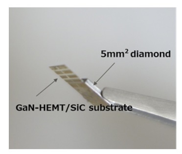
Figure 4: A GaN-HEMT/SiC substrate with diamond bonded using this technology
Results
Thermal resistance, which expresses how difficult it is for heat to pass through something, was measured in samples that were bonded at room temperature, and the SiC/diamond interface was found to have an extremely low thermal resistance of 6.7 x 10⁻⁸ m2K/W (square-meter kelvins per watt). Simulations using this measured parameter showed that this technology would significantly reduce thermal resistance of 200W-class devices, to 61%(5) (Figure 5). Use of this technology promises GaN-HEMT power amps for transmitters with even higher power output. When used in systems such as weather radars, GaN-HEMT power amps for transmitters could be expected to increase the radar's observable range by a factor of 1.5. This would allow for quicker detection of the cumulonimbus clouds that can produce sudden rainstorms, and contribute to a safer and more secure society in terms of disaster readiness.
http://www.acnnewswire.com/topimg/Low_FujitsuSiCFig5.jpg
Figure 5: Simulated comparison of heat in 200W-class GaN-HEMT power amps
Future Plans
Fujitsu and Fujitsu Laboratories plan to assess the thermal resistance and output performance of GaN-HEMT power amps that use this technology, and aim to implement it in high-output, high-frequency GaN-HEMT power amps in fiscal 2020, with use in applications for weather radars and 5G wireless communications systems.
(1) Silicon Carbide (SiC)
A material with relatively good thermal conductivity, about 420 watts per meter per kelvin (W/mK), used for substrates on which GaN-HEMT crystals are grown.
(2) Gallium nitride (GaN)
A wide band-gap semiconductor material that operates with a higher breakdown-voltage than semiconductor technologies based on previous materials, such as silicon (Si)- or gallium-arsenide (GaAs)-based technologies.
(3) High electron mobility transistor (HEMT)
A field-effect transistor that takes advantage of operation of the electron layer at the boundary between semiconductor materials with different bandgaps, which is relatively rapid compared to that within conventional semiconductors. Invented in 1980 by Fujitsu, this technology is currently used in a number of IT applications, including satellite transceivers, cellular equipment, GPS-based navigation systems, and broadband wireless networking systems.
(4) Room-temperature bonding
A technology in which surfaces of different materials are cleaned in a vacuum by an argon beam and bonded at room temperature. Also known as surface activated bonding. This can bond materials that have different coefficients of thermal expansion.
(5) Thermal resistance reduced to 61%
Equivalent to an 80degC reduction in surface temperature in a 200-W class device.
About Fujitsu Laboratories
Founded in 1968 as a wholly owned subsidiary of Fujitsu Limited, Fujitsu Laboratories Ltd. is one of the premier research centers in the world. With a global network of laboratories in Japan, China, the United States and Europe, the organization conducts a wide range of basic and applied research in the areas of Next-generation Services, Computer Servers, Networks, Electronic Devices and Advanced Materials. For more information, please see: http://www.fujitsu.com/jp/group/labs/en/.
Contact:Fujitsu Laboratories Ltd.
Devices & Materials Laboratory
E-mail: next-press@ml.labs.fujitsu.com
Fujitsu Limited
Public and Investor Relations
Tel: +81-3-6252-2176
URL: www.fujitsu.com/global/news/contacts/
Source: Fujitsu Ltd
Sectors: Electronics
Copyright ©2025 JCN Newswire. All rights reserved. A division of Japan Corporate News Network. |