|
Fujitsu Successfully Grows Diamond Film to Boost Heat Dissipation Efficiency of GaN HEMT
Newly-innovated design reduces heat generation by 40%, enabling smaller radar systems
TOKYO, Dec 05, 2019 - (JCN Newswire) - Fujitsu Limited and Fujitsu Laboratories Ltd. have successfully developed the world's first technology for growing a diamond film with highly-efficient heat dissipation on the surface of gallium nitride (GaN)(1) high electron mobility transistors (GaN HEMTs)(2), which are used in power amplifiers for technologies like weather radars and communications equipment. The new design reduces the amount of heat generated by the devices during operations by 40%, leading to simplification of the cooling system and making it possible to miniaturize radar systems that rely on GaN HEMTs. This improvement to the design will make it significantly easier to install larger numbers of the devices for applications including improved weather forecasting and 5G communications.
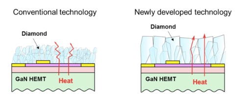 | | Fig. 1 Cross-sectional view of conventional and newly developed diamond film |
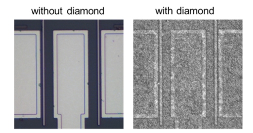 | | Fig. 2 Top view of GaN HEMT |
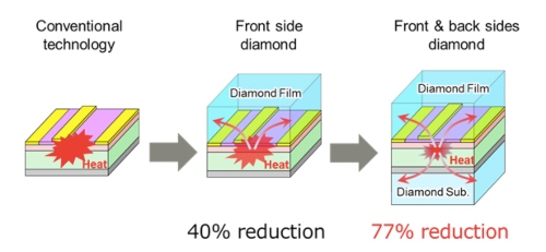 | | Fig. 3 Heat-spreading method and heat dissipation efficiency |
This research was partially supported by the Innovative Science and Technology Initiative for Security, established by the Acquisition, Technology & Logistics Agency (ATLA) of the Japanese Ministry of Defense.
Going forward, Fujitsu aims to commercialize its new high-heat-dissipation GaN HEMT amplifiers in fiscal 2022 for use in weather radar systems and next-generation wireless communication systems.
The details of the technology and related research will be presented at the International Conference on Materials Science "2019 MRS FALL MEETING & EXHIBIT" in Boston, USA, from December 1 (Sunday) to December 6 (Friday).
Development Background
In recent years, GaN HEMTs have been widely used as transistors for high-frequency amplifiers in weather radar and wireless communications. In the future, achieving breakthroughs in areas like the highly accurate observation of localized torrential downpours and the creation of a stable millimeter-wave high-speed communication environment for 5G communications will make it necessary to increase the number of radars and base stations deployed in the world by a considerable degree.
Limitations inherent to existing designs continue to prevent an increase in the number of installations, however. The transistors used in radar systems have higher output power due to the need to operate at longer distances, which increases the amount of heat they generate. Cooling equipment is required because of the performance degradation caused by overheating. This remains expensive, and the large size of the entire system, including the cooling apparatus, limits the installation location, making simplification and miniaturization of the cooling equipment an important challenge for designers.
Challenges
One possible way to reduce the size and complexity of the cooling system is to increase heat dissipation efficiency by covering not only the back surface of the GaN HEMT but also the front surface with a diamond film. This diamond film, which possesses excellent heat dissipation properties, would effectively lower the internal temperature of the GaN HEMT. In order to achieve this effect, however, a diamond crystal with large grain size is required to pass heat efficiently so that heat does not accumulate inside the diamond. A high temperature of about 900 degC is usually required to grow such a diamond film, which unfortunately destroys the GaN HEMT underlying the diamond growth. When a diamond film is grown at low temperature (~ 650degC) at which the GaN HEMT is not destroyed, the resulting reduction in thermal energy given to the methane gas used to create the diamond means that the growth of the diamond is incomplete. Using the low-temperature method, it is only possible to grow microscopic diamond particles (or nanodiamonds) of several hundred nanometers or less. Furthermore, each particle becomes an aggregate of crystals facing different directions, which inhibits efficient heat transfer between particles (Figure 1).
About the Newly Developed Technology
To address this challenge, Fujitsu has developed a technology for growing a highly heat-spreading diamond film at low temperatures (about 650 degC) where transistors are not destroyed, and in a world-first, succeeded in demonstrating the operation of a GaN HEMT with a highly heat-spreading diamond film on its surface.
To grow the diamond film with this method, nanodiamond particles with a diameter of several nanometers are placed on the entire surface of the device. The nanodiamond particles are then exposed to methane gas with high thermal energy to convert the carbon contained in the methane gas into diamond, which can then be incorporated into the particles. Carbon, with its high energy, is selectively incorporated into diamonds that point in a particular direction, allowing diamonds that point in the same direction to bond together and grow.
Focusing on the fact that the thermal energy given to methane varies depending on the pressure and the concentration of methane gas during diamond growth, Fujitsu discovered that nanodiamond particles oriented in a specific direction can be selectively enlarged at low temperatures. This makes it possible to convert a nanodiamond into a micrometer-sized diamond 1000 times larger (Figure 2). As a result, heat can easily pass through the diamond and the GaN HEMT can dissipate heat efficiently.
Outcome
By using the newly developed technology, the amount of heat generated during GaN HEMT operation is reduced by approximately 40% compared to without diamond film, and the temperature can be lowered by 100 degC or more. Furthermore, by combining the heat dissipation from the backside of the GaN HEMTs with single-crystal diamond developed by Fujitsu and silicon carbide bonding technology at room temperature (3), the front and back sides of the GaN HEMTs can be covered with a diamond film, which is expected to reduce heat generation by approximately 77% (Figure 3).
This enables the use of small cooling devices for high-performance radar systems that previously required large cooling devices, thereby saving space and making it easier to install a large number of units demanded for advanced weather forecasting and communications technologies.
Future Plans
Fujitsu aims to commercialize high-heat-dissipation GaN HEMT amplifiers in fiscal 2022 for use in weather radar systems and next-generation wireless communication systems.
(1) Gallium nitride (GaN)
A wide band-gap semiconductor material that features a higher breakdown-voltage (threshold) than conventional semiconductor materials, such as silicon (Si)- or gallium-arsenide (GaAs).
(2) High electron mobility transistor (HEMT)
A field-effect transistor that takes advantage of operation of the electron layer at the boundary between different semiconductor materials that is relatively rapid compared to that within conventional semiconductors. Fujitsu led the industry with its development of HEMT technology in 1980, and the technology now underpins much of today's fundamental IT infrastructure, including satellite transceivers, wireless equipment, GPS-based navigation systems, and broadband wireless networking systems.
(3) Room Temperature Bonding
A technology in which surfaces of different materials are cleaned in a vacuum by an argon beam and bonded at room temperature. Also known as surface activated bonding. This can bond materials that have different coefficients of thermal expansion. https://bit.ly/2RsaH0u
About Fujitsu
Fujitsu is the leading Japanese information and communication technology (ICT) company, offering a full range of technology products, solutions, and services. Approximately 132,000 Fujitsu people support customers in more than 100 countries. We use our experience and the power of ICT to shape the future of society with our customers. Fujitsu Limited (Code: 6702) reported consolidated revenues of 4.0 trillion yen (US $36 billion) for the fiscal year ended March 31, 2019. For more information, please see www.fujitsu.com.
About Fujitsu Laboratories
Founded in 1968 as a wholly-owned subsidiary of Fujitsu Limited, Fujitsu Laboratories Ltd. is one of the premier research centers in the world. With a global network of laboratories in Japan, China, the United States and Europe, the organization conducts a wide range of basic and applied research in the areas of Next-generation Services, Computer Servers, Networks, Electronic Devices, and Advanced Materials. For more information, please see: http://www.fujitsu.com/jp/group/labs/en/.
Fujitsu Limited
Public and Investor Relations
Tel: +81-3-3215-5259
URL: www.fujitsu.com/global/news/contacts/
Fujitsu Laboratories Ltd.
Devices & Materials Laboratory
E-mail: next-press@ml.labs.fujitsu.com
Source: Fujitsu Ltd
Sectors: Electronics
Copyright ©2024 JCN Newswire. All rights reserved. A division of Japan Corporate News Network. |
Latest Release

Fujitsu SX Survey reveals key success factors for sustainability
Apr 23, 2024 10:25 JST
|
Fujitsu and METRON collaborate to drive ESG success: slashing energy costs, boosting productivity with new manufacturing industry solutions
Apr 22, 2024 16:09 JST
| 
NEC Strengthens Commitment to Space Industry with Investment in Seraphim Space Venture Fund II
Apr 22, 2024 15:09 JST
| 
Soft Space Launches the First and Only JCB Payment Gateway in Malaysia
Apr 22, 2024 15:00 JST
| 
TOYOTA GAZOO Racing takes a one-two in Croatian thriller
Apr 22, 2024 10:47 JST
| 
First-ever Mazda CX-80 Crossover SUV Unveiled in Europe
Apr 19, 2024 13:50 JST
|
Fujitsu develops technology to convert corporate digital identity credentials, enabling participation of non-European companies in European data spaces
Apr 19, 2024 10:17 JST
| 
Mitsubishi Heavy Industries and NGK to Jointly Develop Hydrogen Purification System from Ammonia Cracking Gas
Apr 18, 2024 17:01 JST
|
Toyota Launches All-New Land Cruiser "250" Series in Japan
Apr 18, 2024 13:39 JST
|
Fujitsu and Oracle collaborate to deliver sovereign cloud and AI capabilities in Japan
Apr 18, 2024 11:14 JST
| 
Eisai: Research on Treatments for Alzheimer's Disease Based on Its Pathological Mechanisms Recieves Award for Science and Technology (Research Category)
Apr 18, 2024 10:53 JST
| 
All-New Triton Confirmed as First Double-Cab Pickup Truck to Achieve 2024 Five-Star ANCAP Safety Rating
Apr 18, 2024 09:22 JST
|
Eisai's Antiepileptic Drug Fycompa Injection Formulation Launched In Japan
Apr 17, 2024 16:17 JST
| 
Honda Unveils Next-generation EV Series for China
Apr 17, 2024 12:15 JST
| 
Lexus presents Time at the 2024 Milan Design Week
Apr 16, 2024 18:49 JST
| 
Mitsubishi Corporation Announces Participation in a DAC Project in Louisiana, USA
Apr 16, 2024 14:36 JST
|
New circuit challenge for TOYOTA GAZOO Racing
Apr 15, 2024 17:21 JST
|
TOYOTA GAZOO Racing back on asphalt for Croatian challenge
Apr 12, 2024 19:36 JST
|
Heidelberg Materials North America Announces Latest Milestone in Edmonton CCUS Project
Apr 12, 2024 14:39 JST
|
MHIAEL Completes Expansion of the its Nagasaki Plant for Manufacture of Aero Engine Combustors
Apr 11, 2024 18:08 JST
|
More Latest Release >>
|