TOKYO, Mar 15, 2024 - (JCN Newswire) - Hitachi High-Tech Corporation ("Hitachi High-Tech") announced the launch of the LS9300AD, a new system for inspecting the front and backside of non-patterned wafer surfaces for particles and defects. In addition to the conventional dark-field laser scattering detection of foreign material and defects, the LS9300AD is equipped with a new DIC (Differential Interference Contrast) inspection function that enables detection of irregular defects, even shallow, low aspect*1 microscopic defects. LS9300AD has the wafer edge grip method*2 and rotating stage currently used in conventional products to enabling front and backside wafer inspection.With the introduction of LS9300AD, Hitachi High-Tech enables reduced inspection costs and improved yield for semiconductor wafers and semiconductor device manufacturers by providing high-sensitivity and high-throughput detection of low-aspect microscopic defects.
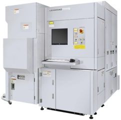 Wafer Surface Inspection System LS9300AD
*1Low-aspect: Generally, aspect ratio refers to the aspect ratio of a rectangle. In this release, "low-aspect" refers to irregularities on the surface and backside of the wafer, microscopic defects with an extremely small ratio of depth to width.*2Wafer edge grip method: A method in which the wafer is fixed only at the edge during inspectionNew Product Development Background
Inspection of non-patterned semiconductor wafers' (before circuit pattern formation) surfaces and backside surfaces has been used in quality assurance during wafers shipment and acceptance, as well as for particles control in various semiconductor device manufacturing processes.Semiconductor wafers manufacturers, use it for quality control to inspect defects and particles that occur during the wafer manufacturing process. In recent years, semiconductor devices have become smaller and more complex, so the size of defects and foreign matter that affect yield in the semiconductor device manufacturing process has become smaller. Due to this, the need for managing all types of defects, including low-aspect microscopic defects on the surface and backside of wafers, is increasing. Responding to the changes in the social environment semiconductor production is expected to increase. To control inspection costs, high-sensitivity and high-throughput inspection equipment is required.
Key New Technologies
In addition to conventional dark-field laser scattering, the LS9300AD has a new DIC optical system that enables both high-sensitivity, high-throughput inspection, and detection of low-aspect microscopic defects.
(1) Built-in DIC Optics
While a dark-field laser irradiates the wafer surface, two beams separated from the DIC laser irradiate two different points on the wafer surface. When there is a difference in height on the wafer surface between the two points irradiated by the DIC laser, the phase contrast of the differential interference signal generated from the difference creates a high-contrast image of wafer surface unevenness. As a result, it is possible to detect the height, area, and position information of low-aspect microscopic defects on the wafer surface, which was difficult to detect using previous techniques.
(2) New DIC-compatible Data Processing System
Along with the DIC optical system, a dark-field laser scattering optical system and a data processing system for defect information obtained through the DIC optical system are installed. This enables simultaneous output of dark-field laser scattering and inspection maps from the DIC optical system, enabling high-sensitivity inspection, even of low-aspect defect data, while maintaining a high inspection speed.
By offering LS9300AD, as well as our metrology systems using electron beam technology and our optical wafer inspection systems, Hitachi High-Tech is working to meet customers' needs in processing, measurement, and inspection throughout the semiconductor manufacturing process. We will continue to provide innovative and digitally enhanced solutions to our products for the upcoming technology challenges, and create new value together with our customers, as well as contributing to cutting-edge manufacturing.
About Hitachi High-Tech Corporation
Hitachi High-Tech Corporation, headquartered in Tokyo, Japan, is engaged in activities in a broad range of fields, including manufacture and sales of clinical analyzers, biotechnology products, and analytical instruments, semiconductor manufacturing equipment and analysis equipment. and providing high value-added solutions in fields of social & industrial infrastructures and mobility, etc.The company's consolidated revenues for FY 2022 were approx. JPY 674.2 billion. For further information, visit https://www.hitachi-hightech.com/global/en/
Contact:
Yuuki MinataniBusiness Planning Dept., Metrology Systems Div., Nano-Technology Solution Business Group, Hitachi High-Tech Corporation
https://www.hitachi-hightech.com/global/en/contactus/#sec-1